Understanding SiP Package Substrate: A Key to Advanced Electronics
This
is no longer an exclusive arena of the semiconductor manufacturers as well as
the specialty design houses only. In
order to internalize their chip design operations, some of the largest
technology players, some of which are not in the hardware business, are hiring
their own semiconductor design teams. High–performance SiP packaging substrates
can be achieved by the right choice of materials, proper layering, and higher
density of wiring, efficient thermal control and signal control. After that, these businesses contract with a
foundry to produce their proprietary SiP package substrate devices, which are
only present in the equipment of the business. This leads to the opportunities
for companies to design new SiP, OSATs and specialized substrate design firms
to come up and offer packaging solutions for these products. These businesses can combine their intellectual
property and physical designs for high-end SiPs through collaboration. There
are main components and peripherals that one needs in the contemporary SIPs if
your company is involved in the generation of IP or offer the service of
component design. The SiP packaged chips
used in medical devices offer high precisions and high reliability of
biosensors, processor and communication modules.

System-in-Package Architecture Design The SiP
package substrate's requirements greatly influence how an SiP architecture is
constructed. Because it is impossible to obtain the appropriate parts from
other suppliers, they are typically used for specialized applications and uses.
In this case, multiple chips can be combined into a single chip. Additionally,
it is anticipated that specialty functions can be integrated in a variety of
ways. It might be particularly mandatory to monitor package performance
including the distribution of currents for instance.
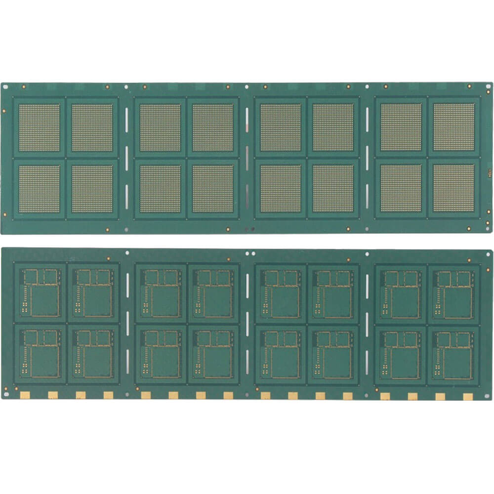
All of the aforementioned architectures can be made proprietary, as is evident from the developed architecture. Architecture of the System In order to interface with peripherals and perform fundamental arithmetical and logical operations, the SoC/SiP package substrate design necessitates certain essential components. The SiP packaging substrate carries and connects chips, passive components, and other electronic components with various functions. Compared with single-chip substrate packaging (BGA, QFP), SiP is increasing the density of the substrate connections, better electrical performance, and higher thermal requirements to meet. As a result, the construction of the SiP packaging substrate involves a number of technologically advanced stages. The SiP packaging substrate is the heart of SiP technology and is subject to a number of manufacturing procedures and technical parameters. High–performance SiP packaging substrates can be achieved by the right choice of materials, proper layering, and higher density of wiring, efficient thermal control and signal control.
System-in-Package (SiP) package substrates are vital in integrating multiple chips or components into a single, compact package. This technology saves a lot of space by combining different functions like sensors, processors, and memory into one unit. The reliability of the entire system is ensured by SiP substrates' excellent electrical connections, thermal management, and mechanical support. SiP packaging, which is prevalent in smartphones, wearables, and Internet of Things (IoT) devices, contributes to the supply of smaller, more powerful electronics. SiP substrates are essential for enabling the next generation of high-performance, miniaturized electronic products as consumer devices become increasingly complex.
Follow our Facebook and Twitter for more information about our product.


Comments
Post a Comment