Get to Know About HDI PCB
High-Density Interconnector is
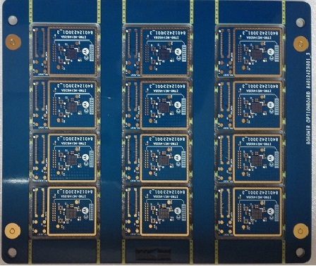
referred to as HDI. HDI PCB Manufacturing contains
smaller vias; fewer capture pads, and a greater connection pad density. They
also have finer gaps and lines. It helps make the instrument smaller and
lighter while enhancing electrical performance. HDI PCB is the ideal option for
pricey laminated boards with a high layer count.
To fulfill the electrical needs of
high-speed communications, the board should have a range of features, including
high-frequency transmission capabilities, impedance control, decreased
redundant radiation, etc. Due to arrays and electronic component reduction, the
board's density must be enhanced. The board is even offered with outstanding
high density as a consequence of the leadless, fine pitch packaging, and direct
chip bonding assembly procedures.
HDI PCB offers a plethora of
advantages, including high frequency, compact size, and fast speed. It is the
main component of personal computers, mobile phones, and portable computers. At
the moment, HDI PCB is widely employed in various consumer goods, such as MP3
players and gaming consoles.
Using equivalent or minimal
amounts of space, HDI PCBs use the most contemporary technology to increase the
functionality of circuit boards. The tiny semiconductor packages and components
that offer extraordinary attributes in cutting-edge new products like
touchscreen tablets are what are driving the progress in board technology.
High-density features on HDI Boards include laser micro-vias, thin high-performance materials, and tiny
lines. More functions may be performed per unit of the area due to the higher
density. The routing precision needed for high pin-count chips used in mobile
devices and other high-tech goods is provided by these kinds of multifunctional
architectures.

Owing to the tiny pads and fine pitch of the circuitry on the circuit board, the location of the components on the board demands higher precision than a normal board design. Leadless chips need special soldering techniques, extra assembly, and repair processes. The HDI circuitry is thinner and lighter; therefore the PCBs may fit into tighter locations and have less mass than traditional PCB designs during HDI PCB Manufacturing. Even the smaller size and lighter weight show that there is a decreased chance of getting hurt by mechanical shocks.


Comments
Post a Comment