High-Density Interconnect (HDI) PCBs: Lightweight, Compact, and Reliable Solutions
Miniaturized
electronic circuit boards are used in various industries: consumer electronics
and communication systems, automotive & aerospace industry & health
care & several other applications. In all these industries, HDI circuit boards or high-density interconnects (HDI PCBs) are of immense value. HDI
technology shall allow the designing and manufacturing of products with low
form factor at nearly the same cost of manufacturing as the standard products
with the same quality, performance, and board reliability.
High-Density
PCBs
High
density of placements of components and / or denser interconnection provided on
any printed circuit board makes it a high density PCB or high density
interconnect PCB. These PCBs provide even more wiring density per unit area
than the previously used PCBs.
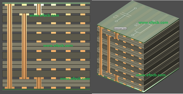
High-density
PCBs consist of:
- Microvias
- Blind and
buried vias
- Layers with
through vias
- coreless
construction with pairs of layers
- An
assortment of coreless constructions with layer pairs
- This means
having no substrate construction to create any form of electrical
connections.
- More of
these interconnections
New
high-density boards are dense and create a new set of rules that define smaller
dimension boards, pads, vias, spaces, and trace width. Due to the dense wiring
pattern in the HDI boards, they are classified as lightweight, miniaturized
circuit boards having less number of layers. The potential of saving PCBs
within a particular product is worthwhile to substitute a few PCBs with an HDI
board.
Advantages
of HDI PCBs
High-density
printed circuit boards are widely used in portable electronics like touch
panels, mobile phones, tablets, PC, digital cameras, laptops, etc High density
interconnect boards are tinier in size compared to regular boards but they
don’t in any way affect the efficiency of the board. The advantages of
HDI PCBs are:
Light
weight and compact sizing – The use of more components on
both sides of HDI circuit boards results into more compact and lighter
PCBs with additional function.
Multiple
boards - With the help of HDI technology, the amount of
the raw material, the number of layers and sometimes even the number of boards
can be less, which creates over cost effect.
Minimized cost and High Density –This shows that the performance increases with increased reliability in HDI boards due to closer components & high transistors per unit area. Compared with other printed circuit board designs, there are relatively fewer signal integrity problems, and a considerable reduction in crossing delays, lost signals, etc. Micro vias also have a tremendously transformative effect as compared to through holes on the reliability of the HDI board because of the small aspect ratio of micro vias and their superior fabrication.

The time to market – The manufacturing of PCBs for the HDI circuit boards also offers remarkable design for productions here the time for market is reduced considerably. In addition, / with HDI boards/ design and testing is also accelerated.”


Comments
Post a Comment